This article needs additional citations for verification. (November 2017) |

In a computer system, a chipset is a set of electronic components on one or more integrated circuits that manages the data flow between the processor, memory and peripherals. The chipset is usually found on the motherboard of computers. Chipsets are usually designed to work with a specific family of microprocessors. Because it controls communications between the processor and external devices, the chipset plays a crucial role in determining system performance. Sometimes the term "chipset" is used to describe a system on chip (SoC) used in a mobile phone.[1][2]
Computers
[edit]In computing, the term chipset commonly refers to a set of specialized chips on a computer's motherboard or an expansion card. In personal computers, the first chipset for the IBM PC AT of 1984 was the NEAT chipset developed by Chips and Technologies for the Intel 80286 CPU.


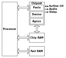
In home computers, game consoles, and arcade hardware of the 1980s and 1990s, the term chipset was used for the custom audio and graphics chips. Examples include the Original Amiga chipset and Sega's System 16 chipset.
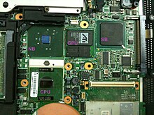
In x86-based personal computers, the term chipset often refers to a specific pair of chips on the motherboard: the northbridge and the southbridge. The northbridge links the CPU to very high-speed devices, especially RAM and graphics controllers, and the southbridge connects to lower-speed peripheral buses (such as PCI or ISA). In many modern chipsets, the southbridge contains some on-chip integrated peripherals, such as Ethernet, USB, and audio devices.
Motherboards and their chipsets often come from different manufacturers. As of 2021[update], manufacturers of chipsets for x86 motherboards include AMD, Intel, VIA Technologies and Zhaoxin.
In the 1990s, a major designer and manufacturer of chipsets was VLSI Technology in Tempe, Arizona. Some of their innovations included the integration of PCI bridge logic, the GraphiCore 2D graphics accelerator and direct support for synchronous DRAM, the forerunner of DDR SDRAM memory.
The Apple Macintosh SE, Macintosh II and later the Quadras series used chipsets from VLSI Technology, even though they were ASICs designed by Apple. After the switch to PowerPC, Apple used various ASIC suppliers for their chipsets such as VLSI technology, Texas Instruments, LSI Logic or Lucent Technologies (later known as Agere Systems). When Apple switched to Intel they used traditional PC chipsets.
In the 1980s, Chips and Technologies pioneered the manufacturing of chipsets for PC-compatible computers. Computer systems produced since then often share commonly used chipsets, even across widely disparate computing specialties. For example, the NCR 53C9x, a low-cost chipset implementing a SCSI interface to storage devices, could be found in Unix machines such as the MIPS Magnum, embedded devices, and personal computers.
Move toward processor integration in PCs
[edit]
Traditionally in x86 computers, the processor's primary connection to the rest of the machine was through the motherboard chipset's northbridge. The northbridge was directly responsible for communications with high-speed devices (system memory and primary expansion buses, such as PCIe, AGP, and PCI cards, being common examples) and conversely any system communication back to the processor. This connection between the processor and northbridge is commonly designated the front-side bus (FSB). Requests to resources not directly controlled by the northbridge were offloaded to the southbridge, with the northbridge being an intermediary between the processor and the southbridge. The southbridge handled "everything else", generally lower-speed peripherals and board functions (the largest being hard disk and storage connectivity) such as USB, parallel and serial communications. In 1990s and early 2000s, the interface between a northbridge and southbridge was the PCI bus.[3]
Before 2003, any interaction between a CPU and main memory or an expansion device such as a graphics card(s) — whether AGP, PCI or integrated into the motherboard — was directly controlled by the northbridge IC on behalf of the processor. This made processor performance highly dependent on the system chipset, especially the northbridge's memory performance and ability to shuttle this information back to the processor. In 2003, however, AMD's introduction of the Athlon 64 series of processors[4] changed this. The Athlon 64 marked the introduction of an integrated memory controller being incorporated into the processor itself thus allowing the processor to directly access and handle memory, negating the need for a traditional northbridge to do so. Intel followed suit in 2008 with the release of its Core i series CPUs and the X58 platform.
In newer processors integration has further increased, primarily through the inclusion of the system's primary PCIe controller and integrated graphics directly on the CPU itself. As fewer functions are left un-handled by the processor, chipset vendors have condensed the remaining northbridge and southbridge functions into a single chip. Intel's version of this is the "Platform Controller Hub" (PCH) while AMD's version was called Fusion Controller Hub (FCH). The PCH is still called a chipset.[5] This is an enhanced southbridge for the remaining peripherals—as traditional northbridge duties, such as memory controller, expansion bus (PCIe) interface and even on-board video controller, are integrated into the CPU die itself (the chipset often contains secondary PCIe connections though). However, the Platform Controller Hub was also integrated into the processor package as a second die for mobile variants of the Skylake processors.[6]
AMD's FCH has been discontinued since the release of the Carrizo series of CPUs as it has been integrated into the same die as the rest of the CPU.[7] However, since the release of the Zen architecture, there's still a component called a chipset which only handles relatively low speed I/O such as USB and SATA ports and connects to the CPU with a PCIe connection. In these systems all PCIe connections are routed directly to the CPU.[8] The UMI interface previously used by AMD for communicating with the FCH is replaced with a PCIe connection. Technically the processor can operate without a chipset; it only continues to be present for interfacing with low speed I/O.[9] AMD server CPUs adopt a self contained system on chip design instead which doesn't require a chipset.[10][11][12]
The northbridge to southbridge interconnect interfaces used now are DMI (Intel) and UMI (AMD). These can also be used for connecting from a processor to a chipset.
See also
[edit]- Acer Laboratories Incorporated
- Comparison of Nvidia nForce chipsets
- List of AMD chipsets
- List of ATI chipsets
- List of Intel chipsets
- Northbridge
- Redpine Signals
- Silicon Integrated Systems
- Southbridge
- Very-large-scale integration or VLSI
- VIA chipsets
Notes
[edit]- ^ "Qualcomm Snapdragon 8 Gen 3 review: I finally don't feel the need to upgrade". 20 January 2024.
- ^ "Qualcomm Announces Snapdragon 8s Gen 3: A Cheaper Chip for Premium Phones".
- ^ Schmid, Patrick (16 July 2002). "Chipset Basics: Meaning And Functions". Tom's Hardware. Purch. Retrieved 14 June 2018.
- ^ Wasson, Scott (23 September 2003). "AMD's Athlon 64 processor". The Tech Report. Retrieved 5 December 2022.
- ^ "MSI Z790 motherboards reportedly failing with cracked PCH chipset — a manufacturing error may have affected a few hundred units (Updated)". 2 April 2024.
- ^ Shimpi, Anand Lal (9 June 2013). "The Haswell Ultrabook Review: Core i7-4500U Tested". AnandTech. Retrieved 5 December 2022.
- ^ "AMD at ISSCC 2015: Carrizo and Excavator Details".
- ^ "AMD Zen 4 Ryzen 9 7950X and Ryzen 5 7600X Review: Retaking the High-End".
- ^ "The AMD Zen and Ryzen 7 Review: A Deep Dive on 1800X, 1700X and 1700".
- ^ "4th Gen AMD EPYC Processor Architecture" (PDF). AMD. Retrieved 3 November 2024.
- ^ Kennedy, Patrick (8 April 2019). "Supermicro M11SDV-4C-LN4F Review mITX AMD EPYC 3151 Platform". ServeTheHome. Retrieved 18 August 2024.
- ^ Cutress, Andrei Frumusanu, Dr Ian. "AMD 3rd Gen EPYC Milan Review: A Peak vs Per Core Performance Balance". www.anandtech.com. Retrieved 18 August 2024.
{{cite web}}: CS1 maint: multiple names: authors list (link)